Computer Science 281
|
 |
Project 2
DSCPU
The Arithmetic and Logic Unit (ALU)ALU Description
The following ALU description specifies an Arithmetic and Logic Unit that can serve the needs of the DSCPU. It supports 10 operations (add, sub, shl, rotl, shr, rotr, and, or, xor, and not) in a combinational circuit that calculates an 8-bit output based on either 1 or 2 8-bit inputs and a 4-bit input specifying the ALU operation to perform. The ALU also computes four flags bits, C, V, N, and Z.
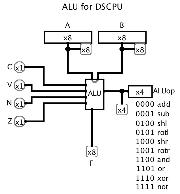
See the Logisim top level design below for a pictorial representation of the interface to the ALU.
Flag Bits
Status flags given as follows: Carry flag. This bit reflects the result of the carry out of the last operation. If data is treated as unsigned and the operation is arithmetic, this bit indicates the carry out (or borrow for subrtract) of the last operation. For shift and rotate operations, this bit is the bit that was shifted or rotated out of the result. For logic operations, this bit is always 0. Overflow flag. For arithmetic operations, this bit is asserted if the carry into the most significant bit of the result does not equal the carry out of the most significant bit of the result of the last executed arithmetic operation. It is 0 if the carry into of the most significant bit equals the carry out of the most significant bit of the result of the last arithmetic operation. For all other operations (shift, rotate, and logical operations) this bit is always 0. Negative flag. This bit is updated as a result of all arithmetic, shift, and logic operations. If the result of an operation has its most significant bit asserted, then N is asserted. If the result of an operation does not have the most significant bit asserted, then N is 0. Zero flag. This bit is updated as a result of all arithmetic, shift, and logic operations. If the result of an operation is zero, then Z is asserted. If the result of an operation is not zero, then Z is 0. ALU Operations
In the following table, an A operand refers to a 16-bit memory address and is composed of the two bytes (MSB followed by LSB) following the opcode in memory. An I operand refers to an 8-bit immediate value and is found in the byte immediately following the opcode in memory.
Operation ALU op
(binary)Semantics F = A + B; CVNZ update F = A + ~B + 1; CVNZ update F = A shifted left one bit position, zero fill in lsb; CVNZ update F = A rotated left one bit position; CVNZ update F = A shifted right one bit position, zero fill in msb; CVNZ update F = A rotated right one bit position; CVNZ update F = A & B; CVNZ update {bitwise AND} F = A | B; CVNZ update {bitwise OR} F = A ^ B; CVNZ update {bitwise XOR} F = ~A ; CVNZ update {bitwise complement} Assignment
Using the Logisim digital logic design and simulator package, design and implement the DSCPU ALU. You must only use component elements from the "Base" and "Gates" categories, and you must use clean hierarchical design.
Top-level Interaction
- Your design should structure the ALU itself as a subcircuit.
- From the "main" circuit, you should have 8-bit wide pin inputs for the A and B operands and a 4-bit wide pin input for the ALUop. Each of these should also include a hexadecimal probe to show the values on the input wires.
- Your main circuit should have 5 outputs, displayed through probes. The ALU result is F and is 8 bits wide, and each of the Flag bits are 1 bit wide and should be labeled C, V, N, and Z (_in that order_)
- See the picture below of the solution that I have designed.
Deliverables
Your submission will be a Logisim circuit file. These files end in a .circ extension. This file should be comatible with version 2.1.5 of the Logisim software. You will email the file to me by the due date. As long as the top level follows the specification given above, the only documentation required is a short description of the design of each of your subcircuits, along with a list of the more primitive subcircuits used by each one.
Hints
- Within the ALU circuit itself, my top level decompostion consists of 4 circuits:
- an add/sub unit responsible for both addition and subtraction operations and having 2 8-bit inputs and a 1-bit control input that, when 0 performs addition and when 1 performs subtraction.
- A "left" unit responsible for both shit left and rotate left, having 2 8-bit inputs and a 1-bit control input (for shift versus rotate).
- A "right" unit responsible for both shit right and rotate right, having 2 8-bit inputs and a 1-bit control input (for shift versus rotate).
- A logic unit responsible for and, or, xor, and not, having 2 8-bit inputs and a 2-bit control input to select the suboperation.
- Often in digital logic design, we let the inputs derive outputs for multiple operations in parallel, and then simply multiplex to select the output desired for the current operation.
- Some of the subcircuits my own solution utilized include both 2-to-1 and 4-to-1 multiplexers in 1-bit wide and 8-bit wide varieties.
- Subtraction can be handled by having both the positive form of the B operand and its 1-s complement available as input to an adder. We can use a multiplexer to select which we want to flow into the adder unit. When subtraction is occuring, we also need to add one to get the two's complement, but this can be neatly handled by using the carry-in bit of the adder.
- The computation of Z and N must happen (in the same way) for all 10 operations. It makes sense to do this outside of the 4 top-level subcircuits after the final output F has been determined. The Carry and Overflow, however, are specific to the category of ALU operation and are better handled within each of the top-level subcircuits.